New York Center for Research, Economic Advancement,
Technology, Engineering and Science
Albany 300mm Fab Facilities and Technology
Brett Baker-O’Neal (bbaker-oneal@ny-creates.org), Frank Tolic (ftolic@ny-creates.org)
2
SUNY RF / NY CREATESConfidential
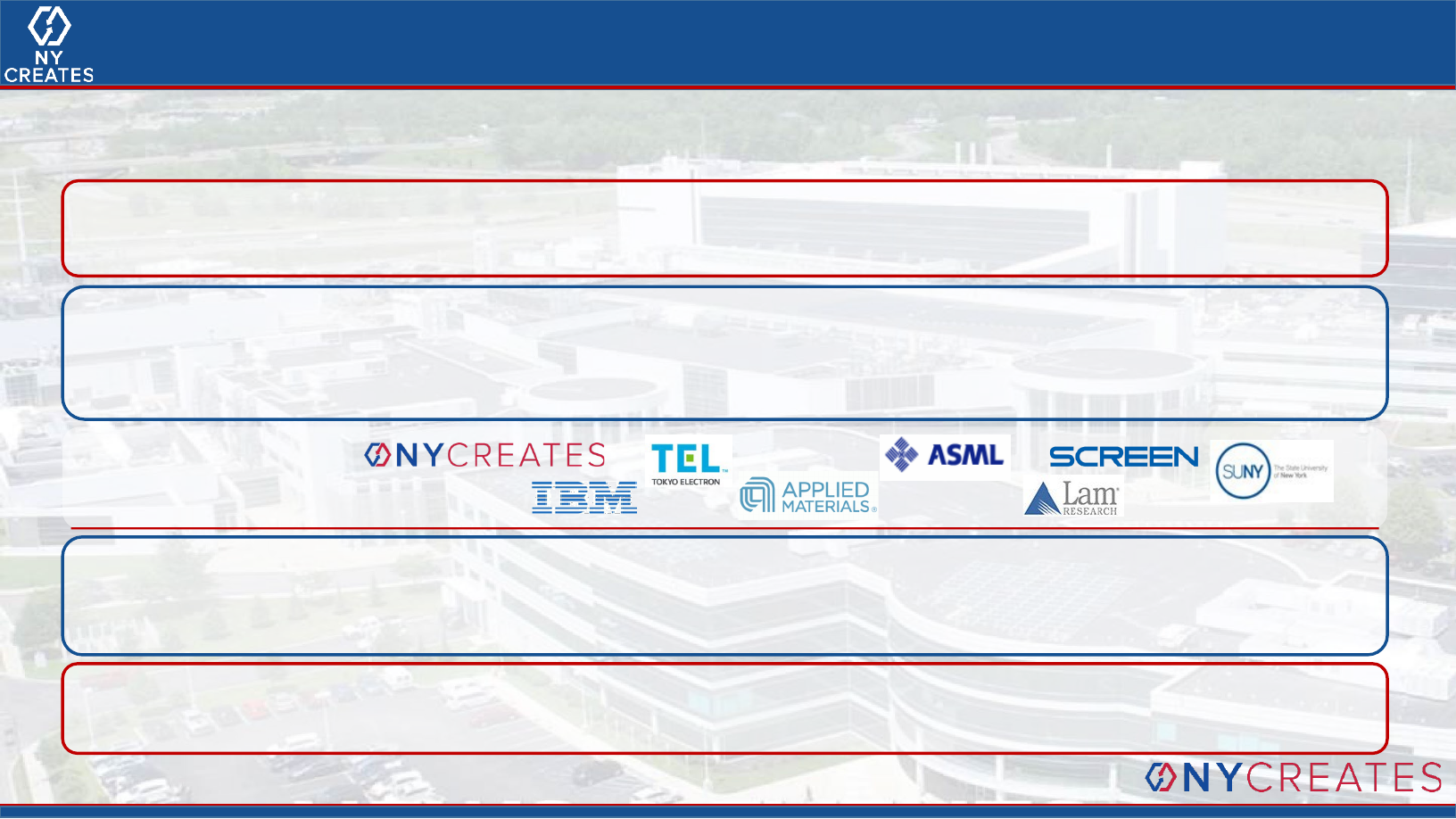
NY CREATES
New York Center for Research, Economic Advancement,
Technology, Engineering and Sciences
• NY CREATES accelerates next generation semiconductor technology
research and develops the workforce to support the innovation economy
Mission
Infrastructure
and Ecosystem
• 20+ year history of public-private R&D partnerships & investment
• Capital investment in excess of $15 billion
• 100k+ sq ft of 300mm cleanroom fabs – CSR, AMAT META, TEL TTCA
Technology
Enablement
Engagement
Models
Partners
and more
• Logic node range: 2nm nanosheet transistors 65nm Photonics derivatives
• Novel memory, neuromorphic computing, quantum computing
• Heterogeneous Integration and Packaging
• Development Agreement, Development Associates, Wafer Processing
• Custom Fabrication, Test Evaluation, Product and Services Purchase
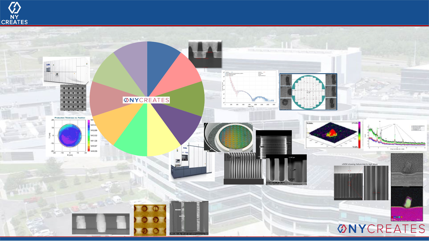
World-Class Capabilities at NY CREATES
ASML TWINSCAN NXE:3400
300mm Si Fab Capabilities – Ful -flow FEOL and BEOL
Failure Analysis
Inline Metrology and Defectivity
Cu BEOL
C24P48
ASML TWINSCAN NXT:1950i
Heterogeneous Integration (HI) Fab Center
• Fusion Bond, Die-to-Wafer Bond, Temp Bond, Debond
• Post-bond Grind and Bond Test
• Bump Metallization
• TSV integration
Cu bond pads
TEOS / Cu hybrid bond
TSV
Bosch etch
HAR Etch into Oxide
Silicon
Pillar
Etch
AFM
Offline Metrology
XRD
CMP
METALS
METROLOGY
RIE
LITHOGRAPHY
WETS
THERMAL
EUV
INSULATORS
epi
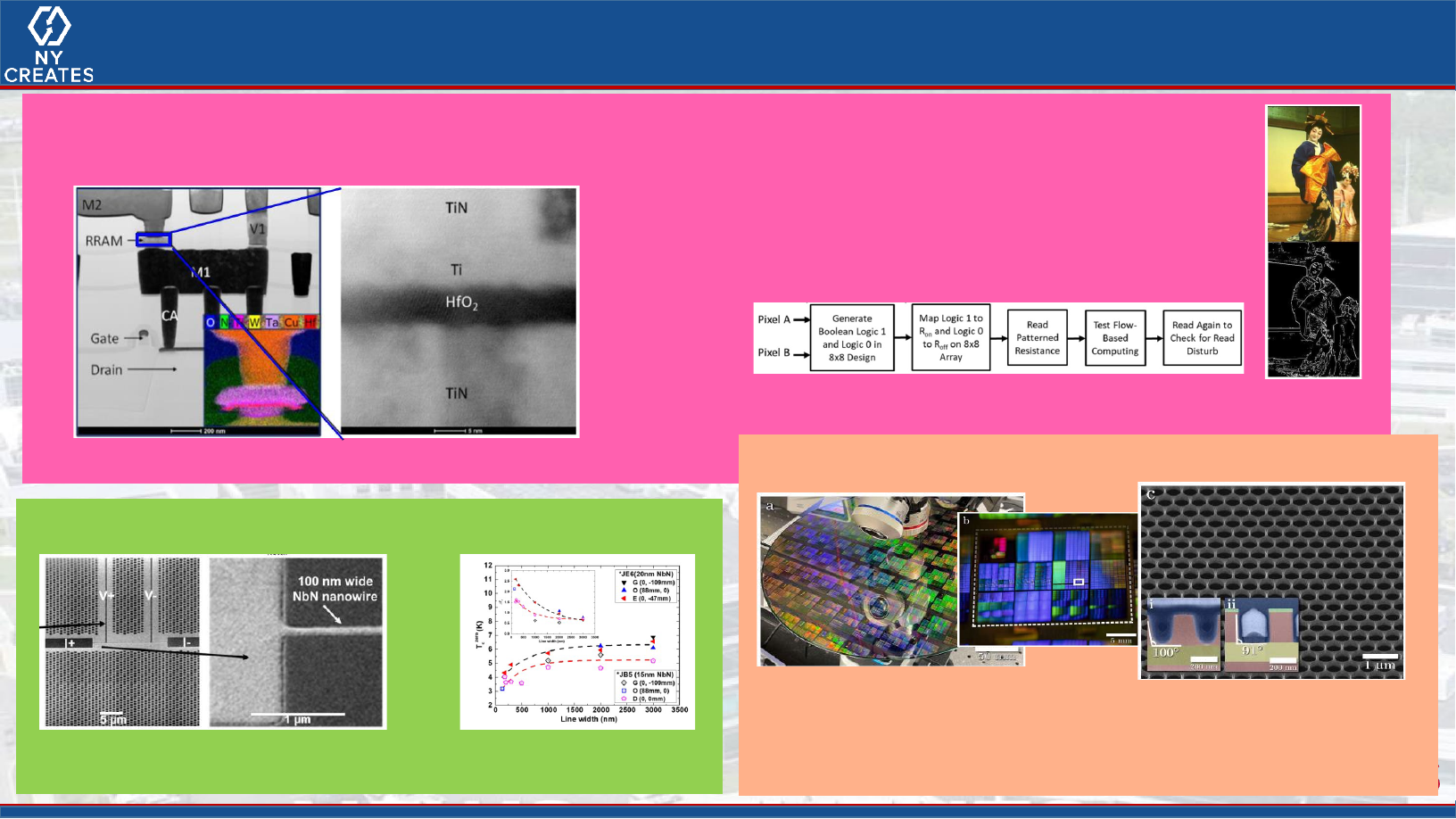
Technology Development at NY CREATES
ReRAM
TEM of 1T1R integration of HfO2 RRAM devices and inset of EDX
compositional analysis of ReRAM stack
J. Hazra, M. Liehr, K. Beckmann, S. Rafiq and N. Cady
2020 IEEE International Integrated Reliability Workshop (IIRW)
NbN devices for 4-probe measurement atcryogenic
temperatures
Cryogenic Tc Measurements
Soumen Kar, et. al., TRANSACTIONS ON APPLIED SUPERCONDUCTIVITY, VOL. 33, NO. 5, AUGUST 2023
Superconducting and Quantum Computing
Photonic Crystal Fabrication
Christopher L. Panuski, Nat. Photon. 16, 834–842 (2022)
Full-wafer photonic crystal
fabrication in an optimized300
mm foundry process. A wafer
contains 64 complete reticles.
Mil ions of inverse designed PhC cavities. The before
(i) and after (i ) false-color (blue: metal l ; red:silicon;
yellow: silicon dioxide; green: etch mask)
transmission electron microscope cross-sections
show how process optimization enables high-quality
PhC lattices.
• CMOS/RRAM Hardware In-memoryComputing
• Used 8x8 1T1R arrays to perform flow-through computing for image
pixel comparison / edge detection.
• Bitwise comparison of pixels results in robust image edge detection in
both simulation and experimentally on 1T1R arrays.
Pixel Comparison in 8x8 1T1R Array
S. Rafiq, J. Hazra, M. Liehr, K. Beckmann, M. Abedin, J.S. Pannu, S.K. Jha, N.C. Cady.
Accepted - IEEE Transactions on Circuits and Systems – April 2021

THANK YOU
Brett Baker-O’Neal, NY CREATES, Development Engineering, bbaker-oneal@ny-creates.org
Frank Tolic, NY CREATES, Business Development, ftolic@ny-creates.org
